MetaRosetta
- Home
- PRODUCT LINE
Key Advantages:
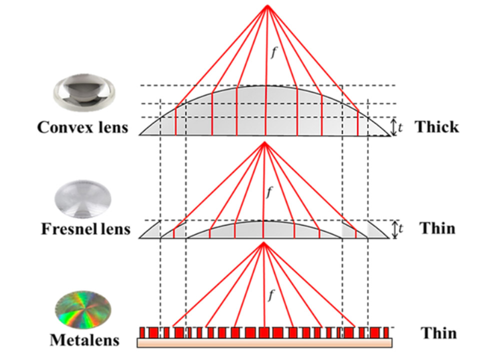
Ultra-Thin: Lens thickness reduced from millimeter scale (mm) to micrometer scale (μm).
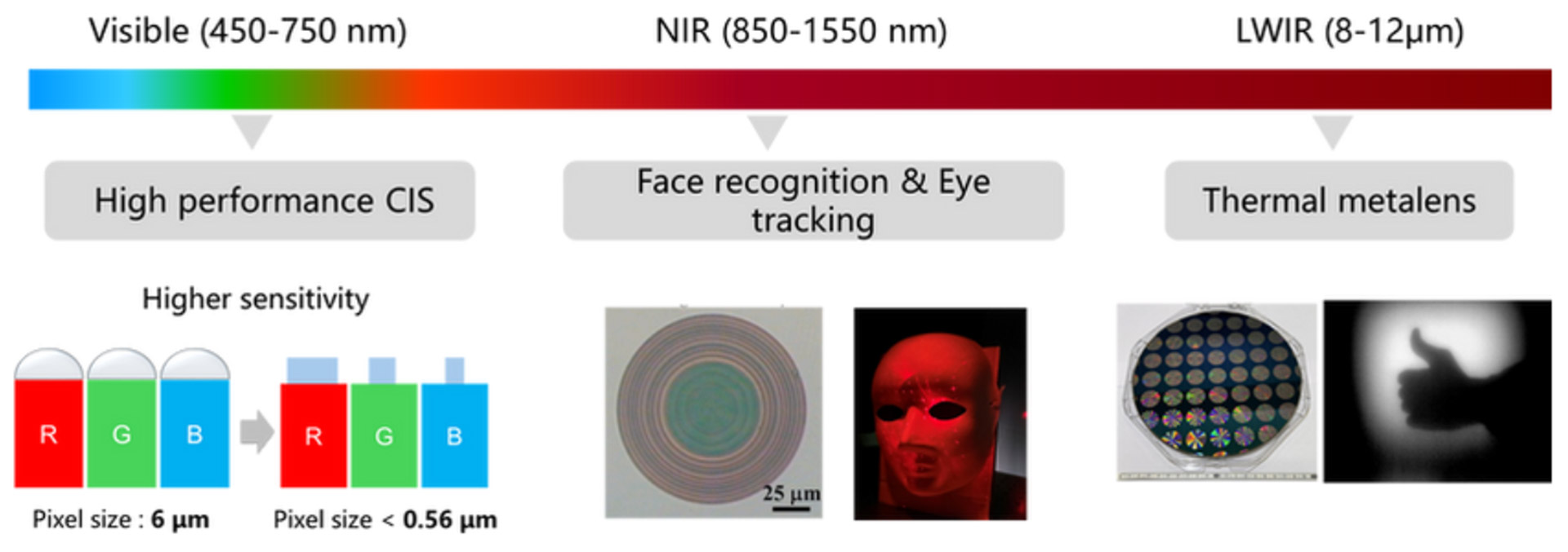
Functional Integration: Achieves complex functions such as chromatic aberration correction, polarization control, and beam shaping on a single flat surface.
Wafer-Level Manufacturing (WLO Ready): Easily integrates with semiconductor processes, lowering costs for large-scale mass production.
Our Strength: Our Metalens IP and design capabilities focus on achieving high efficiency and broadband response, providing downstream partners with optimized optical cores. From bulky to lightweight, from multiple elements to a single piece. Our Metalens IP specializes in nanostructure design, not only miniaturizing complex multi-lens systems but also integrating multiple functions on a single flat surface, bringing lower system costs to your next-generation optical components.